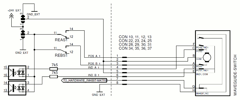
Your sat-nms IO-FEP2 is by factory default configured in that way most of usually used waveguide-switch work: it provides a 24V DC pulse to trigger a switchover of connected waveguide switch. GND is COM in this case. There are some waveguide switches available that work exactly contrary: They need a GND 'pulse' and have 24V DC as COM. Therefore sat-nms IO-FEP2 also provides a solution: It is possible to change polarity of waveguide-switch interfaces in blocks of 4. By that it is possible to e.g. connect 12 'normal' ones and 4 switches with changed polarity. Following picture shows the schematic of a switch interface in standard configuration:
Reconfiguration of polarity will be explained exemplary with the first block of switch interfaces No. 1...4. This correlates to CON10...CON13. Configuration is done by changing solder jumpers.
take care that sat-nms IO-FEP2 is switched off during this modification!
This modification should be carried out by well trained personnel only!
Both solder jumpers are located between CON10/11 and CON12/13. you can easily see this on following picture. We strongly recommend to unplug affected connectors in order to get enough space for working with a soldering-iron.
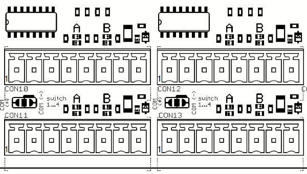
Standard configuration is marked with a little line besides the pads that have to be connected. As you can see on the picture, both jumpers are marked with 'COM (-)' here. A little 'switch 1...4' is marked here too, in order to clarify correlation to affected switch interfaces. To change polarity, you have to connect left and middle pad marked with 'COM (+)' on both jumpers. By this, 24V EXT is connected as COM, GND EXT will be pulse switched to trigger a switchover. It is essentially, that both solder jumpers are always in same configuration, otherwise this interface does not work. Now, switch interfaces #1...#4 are configured with inverted polarity. All others work in 'normal' way if solder jumpers have not been changed here. If you like to connect more waveguide switches with inverted polarity, go ahead comparable to this example. Each 4 interfaces act as one block that might be configured. Following table shows which switch belongs to which block and location of each solder jumper.
| switch-interface No. | location of solder jumper |
|---|---|
| 1, 2, 3, 4 | between CON10/11 and CON 12/13 |
| 5, 6, 7, 8 | between CON22/23 and CON 24/25 |
| 9, 10, 11, 12 | between CON28/29 and CON 30/31 |
| 13, 14, 15, 16 | between CON34/35 and CON 36/37 |