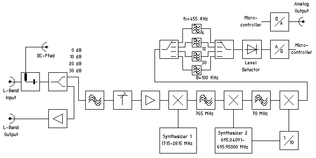
The following block diagram shows the functional blocks of the sat-nms L-Band Beacon Receiver.
The L-band input signal is applied to the SMA connector X1. The receive frequency range is from 950MHz to 2050MHz. A small portion of the input signal is coupled out of the main signal flow, the coupling is compensated by a small amplifier and this signal is provided as a L-band test output signal with the same output level at the L-Band test output SMA connector with the same power level for test and measurement purposes. The L-band signal is filtered within a 950 to 2050MHz filter and then attenuated by a programmable attenuator in steps of 0dB, 10dB, 20dB or 30dB. After this programmable attenuator a first amplifier with approximately 20dB of gain and a noise figure of 3.5dB amplifies the signal for the first down conversion in a 13dBm mixer. This mixer converts the L-band input signal to the first IF of 765MHz by use of a PLL frequency synthesiser. This mixer is highly linear and determines the overall dynamic range of the system.
The 765MHz signal is then filtered by use of two 3-pol. ceramic filters which attenuates the out of receive channel signals. After these two filter stages the 765MHz signal is converted by a second mixer to a 70MHz IF by use of the fractional-N synthesiser. Direct behind the mixer a SAW filter with approximately 300kHz bandwidth is used to filter the 70MHz signal. This filter has a very high Q so that only frequencies inside the bandwidth will be fed to the last mixer circuit.
This mixer converts the 70MHz IF into the final 455kHz IF by use of 1/10 the frequency of the fractional- N synthesiser. The 455kHz IF signal is the fed into a one of four analog multiplexer circuit. Via the internal micro controller the appropriate bandwidth of 6, 12 30 and 100KHz is selectable. The 6, 12 and 30KHz filters are ceramic filters the 100kHz filter is due to the high relative bandwidth a discrete filter with inductors and capacitors. OP-amps behind the filters are used to match the filters with the appropriate impedance and are used to provide almost the same level as at the multiplexer input. In a last gain stage the 455kHz signal is amplified to the appropriate level for the level detector.
The signal level is measured with a logarithmic amplifier. This level detector has a very high dynamic range and is also very linear. Output of the level detector is a D/C voltage proportional to the L-band input power. This voltage is converted into a 16bit digital word by an analogue to digital converter with 16bit resolution.
A on board temperature sensor gives the beacon receiver M&C board the knowledge about the temperature on the RF circuit board and allows fro temperature compensation.
D/C-input to the beacon receiver is +24V/0.5A provided by the M&C board.
There are two D/C-D/C converters on the board to convert the +24V D/C into +6V for the analog +5V supply and the digital +3.3V / +5V. The digital D/C voltage regulator provides a DC_ERROR signal which can be read back to the M&C board.
The 2nd D/C-converter is used for the LNB supply which can be programmed either to 14V or 18V. Furthermore this LNB voltage can be modulated by the Diseq_22kHz signal to provide a DiseqC interface. The DiseqC interface is not implemented in the first design stage but the hardware basis is given with this circuit design and the real DiseqC implementation is later on a question of software in the micro-controller on the beacon receiver M&C board. At the moment only a 22KHz signal is generated if necessary
In cases where no LNB supply is needed the D/C converter can be switched off by the LNC_ON signal.
In order to reduce interference from the micro-controller to the RF part and also to reduce cost on the PC board production the circuit for the monitoring and control of the L-Band beacon receiver is designed on a second printed circuit board.
The main interface to the beacon receiver RF board is via the SPI interface. This means that the analog to digital converter, the temperature sensor and also all monitoring and alarm input and output ports are placed on the RF board and the digital information is routed via the SPI bus to the M&C board and its micro-controller.
In addition to that the following interface is provided, the output of the logarithmic detector provides a analog output voltage which can be used via two interfaces:
This micro-controller controls also the synthesiser and the other hardware selections like bandwidth control. The micro-controller communicates to the to the 'outside world' through two serial communication interfaces. See chapter ' 3 Operation / Remote Control ' for details.