This chapter gives a short overview about some configuration parameters you want to set after you have installed the sat-nms IO-FEP. A complete reference of all available setup parameters is given in chapter 3.4 Installation Parameters .
setting the HPA-mute-matrix
When the connected waveguide switches are equipped with inhibit contacts, it is possible to mute different connected HPA`s while the waveguide-switch is switching. Every of the 10 DIP-switches DIP1...10 represents one HPA #1...10. The numbers written on every DIP-switch belong to the numbers of the waveguide switches. When the switch is in position "on" the HPA mutes, when this waveguide switch switches.
An example: You want to mute HPA #1 when waveguide switch #2 or #4 or #8 changes its condition. Then you have to configure on the DIP-switch DIP1 the switches #2 and #4 and #8 into the "on"-position. All the others have to be in the "off"-position.
The extended version IO-FEP-E has additional DIP-switches DIP11...20. With these switches you select which HPA should mute, when one or more of the waveguide-switches #9...13 is switching. DIP11 represents HPA1, DIP12 HPA2 an so on.
An example: You want to mute HPA #1 when waveguide switch #2 or #9 or #16 changes its condition. Then you have to configure on the DIP-switch DIP1 the switch #2 and on DIP-switch DIP11 the switch #9 and #16 into the "on"-position. All the others have to be in the "off"-position.
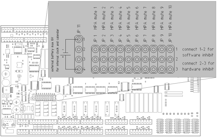
If the connected waveguide-switch is not equipped with inhibit-contacts, the sat-nms IO-FEP nevertheless gives you the possibility to mute the HPA in the switching moment by software. Therefore you have to open the enclosure of the sat-nms IO-FEP and put the Jumper with the number of the HPA in the upper position (pin 1-2) afterwards you have to configure the software-muting-matrix. How to do this is described in chapter 3.4 Installation Parameters . The following picture shows, where you can find JP1...10, the jumpers that define if the inhibit-signal comes from the waveguide-switches or is generated by the processor from the sat-nms IO-FEP.
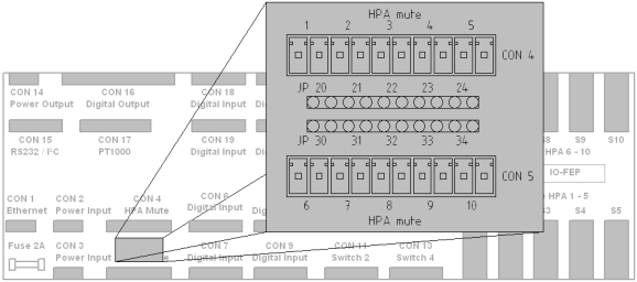
For bypassing the inhibit-switching, you find 2 sockets between CON4 and CON5. Use the "jumper extension" that is shipped with the sat-nms IO-FEP and normal jumpers to bypass the inhibit-outputs. JP20...24 bypasses the inhibit-signal for HPA #1...5, JP30...34 bypasses the inhibit-signal for HPA#6...10. The following picture shows you where to find the sockets.
A T T E N T I O N ! when you bypass the inhibit-outputs, the connected HPA(s) will not mute in case of switching a waveguide-switch! The HPA and the waveguide switch as well might be damaged in this case! Ensure that no waveguide-switch is switched when the inhibit signal is bypassed!
photomos-relay digital outputs
If you don't have some HPA's to mute or don't need all the mute-outputs, you can use them also as digital outputs. Therefore you have to open the enclosure of the sat-nms IO-FEP and put all the jumpers of the outputs, that you want to use this way, in the upper position (pin 1-2). In the second last picture you can see where to find this Jumpers on the PCB of the sat-nms IO-FEP. Dont´t exceed the continuous current limit of 130mA and the continuous voltage of 48V DC. Otherwise the sat-nms IO-FEP might be damaged. If you want to switch inductive loads, don`t forget to add a clamp diode to limit the spike voltages in the switching moment.
digital inputs DIN41...48 on the IO-FEP-E
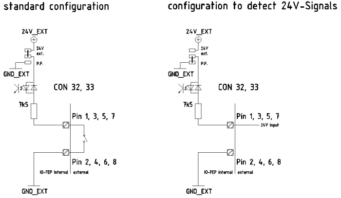
On the extended version IO-FEP-E you can select, if you like to detect potential- free on/off-contacts or if you want to detect a 24V DC Voltage. The factory setting is to detect potential-free contacts, like all the other digital-inputs. If you want to detect 24V DC voltages, you have to do the following procedure: Open the IO-FEP-E's enclosure. Top right you find two opto-coupler with black enclosures (all the others are white). Below these optocouplers you can see two solder-jumpers, as you can see on the following picture. The left one is for DIN41...44, the right one for DIN45...48. Now open the connection of the solder-jumper that belongs to the DIN that you want to change. After that close the connection between the middle and the right-pad (P.F.). The following picture shows you where to find the solder jumpers on the PCB.
The following picture shows how to connect the digital inputs #41...48 in both ways of configuration, and how it works internally.