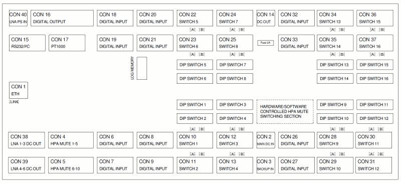
Connector layout sat-nms IO-FEP2:
CON1 LAN
| Pin | Identifier | Description | Type | Remark |
|---|---|---|---|---|
| 1 | TX+ | default Ethernet cabling (10Base-T) | OUT | |
| 2 | TX- | OUT | ||
| 3 | RX+ | IN | ||
| 4 | ||||
| 5 | ||||
| 6 | RX- | IN | ||
| 7 | ||||
| 8 |
CON2 main power input
| Pin | Identifier | Description | Type | Remark |
|---|---|---|---|---|
| 1 | 24V INT | voltage input for IO-FEP2 | DC in | |
| 2 | GND INT | DC in | ||
| 3 | 24V EXT | voltage input for WG Switches etc. | DC in | |
| 4 | GND EXT | DC in |
CON3 backup power input
| Pin | Identifier | Description | Type | Remark |
|---|---|---|---|---|
| 1 | 24V INT | voltage input for IO-FEP2 | DC in | |
| 2 | GND INT | DC in | ||
| 3 | 24V EXT | voltage input for WG Switches etc. | DC in | |
| 4 | GND EXT | DC in |
CON4 HPA mute
| Pin | Identifier | Description | Type | Remark |
|---|---|---|---|---|
| 1 | MUT IN1 | HPA 1 mute in | DC in | |
| 2 | MUT OUT1 | HPA 1 mute out | DC out | |
| 3 | MUT IN2 | HPA 2 mute in | DC in | |
| 4 | MUT OUT2 | HPA 2 mute out | DC out | |
| 5 | MUT IN3 | HPA 3 mute in | DC in | |
| 6 | MUT OUT3 | HPA 3 mute out | DC out | |
| 7 | MUT IN4 | HPA 4 mute in | DC in | |
| 8 | MUT OUT4 | HPA 4 mute out | DC out | |
| 9 | MUT IN5 | HPA 5 mute in | DC in | |
| 10 | MUT OUT5 | HPA 5 mute out | DC out |
CON5 HPA mute
| Pin | Identifier | Description | Type | Remark |
|---|---|---|---|---|
| 1 | MUT IN1 | HPA 6 mute in | DC in | |
| 2 | MUT OUT1 | HPA 6 mute out | DC out | |
| 3 | MUT IN2 | HPA 7 mute in | DC in | |
| 4 | MUT OUT2 | HPA 7 mute out | DC out | |
| 5 | MUT IN3 | HPA 8 mute in | DC in | |
| 6 | MUT OUT3 | HPA 8 mute out | DC out | |
| 7 | MUT IN4 | HPA 9 mute in | DC in | |
| 8 | MUT OUT4 | HPA 9 mute out | DC out | |
| 9 | MUT IN5 | HPA 10 mute in | DC in | |
| 10 | MUT OUT5 | HPA 10 mute out | DC out |
CON6 digital input
| Pin | Identifier | Description | Type | Remark |
|---|---|---|---|---|
| 1 | DIN 1 | digital input | input | |
| 2 | GND | refenece voltage | DC out | |
| 3 | DIN 2 | digital input | input | |
| 4 | GND | refenece voltage | DC out | |
| 5 | DIN 3 | digital input | input | |
| 6 | GND | refenece voltage | DC out | |
| 7 | DIN 4 | digital input | input | |
| 8 | GND | refenece voltage | DC out |
CON7 digital input
| Pin | Identifier | Description | Type | Remark |
|---|---|---|---|---|
| 1 | DIN 5 | digital input | input | |
| 2 | GND | refenece voltage | DC out | |
| 3 | DIN 6 | digital input | input | |
| 4 | GND | refenece voltage | DC out | |
| 5 | DIN 7 | digital input | input | |
| 6 | GND | refenece voltage | DC out | |
| 7 | DIN 8 | digital input | input | |
| 8 | GND | refenece voltage | DC out |
CON8 digital input
| Pin | Identifier | Description | Type | Remark |
|---|---|---|---|---|
| 1 | DIN 9 | digital input | input | |
| 2 | GND | refenece voltage | DC out | |
| 3 | DIN 10 | digital input | input | |
| 4 | GND | refenece voltage | DC out | |
| 5 | DIN 11 | digital input | input | |
| 6 | GND | refenece voltage | DC out | |
| 7 | DIN 12 | digital input | input | |
| 8 | GND | refenece voltage | DC out |
CON9 digital input
| Pin | Identifier | Description | Type | Remark |
|---|---|---|---|---|
| 1 | DIN 13 | digital input | input | |
| 2 | GND | refenece voltage | DC out | |
| 3 | DIN 14 | digital input | input | |
| 4 | GND | refenece voltage | DC out | |
| 5 | DIN 15 | digital input | input | |
| 6 | GND | refenece voltage | DC out | |
| 7 | DIN 16 | digital input | input | |
| 8 | GND | refenece voltage | DC out |
CON10 waveguideswitch 1
Following table shows interface with standard configuration! Refer to chapter Change polarity of waveguide-switch interfaces if you need inverse actuation.
| Pin | Identifier | Description | Type | Remark |
|---|---|---|---|---|
| 1 | POS A 1 | set position A | DC out | |
| 2 | GND_EXT | com | DC out | |
| 3 | POS B 1 | set position B | DC out | |
| 4 | IND A 1 | indication position A | DC out | |
| 5 | GND_EXT | com | DC out | |
| 6 | IND B 1 | indication position B | DC out | |
| 7 | INH 1 | inhibit | DC out | |
| 8 | GND_EXT | inhibit | DC in |
CON11 waveguideswitch 2
Following table shows interface with standard configuration! Refer to chapter Change polarity of waveguide-switch interfaces if you need inverse actuation.
| Pin | Identifier | Description | Type | Remark |
|---|---|---|---|---|
| 1 | POS A 2 | set position A | DC out | |
| 2 | GND_EXT | com | DC out | |
| 3 | POS B 2 | set position B | DC out | |
| 4 | IND A 2 | indication position A | DC out | |
| 5 | GND_EXT | com | DC out | |
| 6 | IND B 2 | indication position B | DC out | |
| 7 | INH 2 | inhibit | DC out | |
| 8 | GND_EXT | inhibit | DC in |
CON12 waveguideswitch 3
Following table shows interface with standard configuration! Refer to chapter Change polarity of waveguide-switch interfaces if you need inverse actuation.
| Pin | Identifier | Description | Type | Remark |
|---|---|---|---|---|
| 1 | POS A 3 | set position A | DC out | |
| 2 | GND_EXT | com | DC out | |
| 3 | POS B 3 | set position B | DC out | |
| 4 | IND A 3 | indication position A | DC out | |
| 5 | GND_EXT | com | DC out | |
| 6 | IND B 3 | indication position B | DC out | |
| 7 | INH 3 | inhibit | DC out | |
| 8 | GND_EXT | inhibit | DC in |
CON13 waveguideswitch 4
Following table shows interface with standard configuration! Refer to chapter Change polarity of waveguide-switch interfaces if you need inverse actuation.
| Pin | Identifier | Description | Type | Remark |
|---|---|---|---|---|
| 1 | POS A 4 | set position A | DC out | |
| 2 | GND_EXT | com | DC out | |
| 3 | POS B 4 | set position B | DC out | |
| 4 | IND A 4 | indication position A | DC out | |
| 5 | GND_EXT | com | DC out | |
| 6 | IND B 4 | indication position B | DC out | |
| 7 | INH 4 | inhibit | DC out | |
| 8 | GND_EXT | inhibit | DC in |
CON14_Power_output
| Pin | Identifier | Description | Type | Remark |
|---|---|---|---|---|
| 1 | 24V EXT | spare output | DC out | |
| 2 | 24V EXT | spare output | DC out | |
| 3 | GND EXT | DC out | ||
| 4 | GND EXT | DC out |
CON15 RS232 I2C
| Pin | Identifier | Description | Type | Remark |
|---|---|---|---|---|
| 1 | RS232 0 TX | RS232 access 0 | output | |
| 2 | RS232 0 RX | input | ||
| 3 | GND INT | DC out | ||
| 4 | RS232 1 TX | RS232 access 1 | output | |
| 5 | RS232 1 RX | input | ||
| 6 | I2C SDA | I²C data | in-/output | inactive |
| 7 | I2C SCL | I²C clock | output | inactive |
| 8 | GND INT | DC out |
CON16 digital out
| Pin | Identifier | Description | Type | Remark |
|---|---|---|---|---|
| 1 | COM 11-13 | input | ||
| 2 | COM | input | ||
| 3 | 11 | switched COM11-13 | output | |
| 4 | COM | output | ||
| 5 | 12 | switched COM11-13 | output | |
| 6 | COM | output | ||
| 7 | 13 | switched COM11-13 | output | |
| 8 | COM | output | ||
| 9 | input 14 | input | ||
| 10 | 14 | switched input 14 | output | |
| 11 | input 15 | input | ||
| 12 | 15 | switched input 15 | output | |
| 13 | input 16 | input | ||
| 14 | 16 | switched input 16 | output |
CON17 external temperature sensors
| Pin | Identifier | Description | Type | Remark |
|---|---|---|---|---|
| 1 | SENS OUT1 | output to PT1000 | DC out | |
| 2 | SENS IN1 | input to PT1000 | DC in | |
| 3 | SENS OUT2 | output to PT1000 | DC out | |
| 4 | SENS IN2 | input to PT1000 | DC in | |
| 5 | SENS OUT3 | output to PT1000 | DC out | |
| 6 | SENS IN3 | input to PT1000 | DC in | |
| 7 | SENS OUT4 | output to PT1000 | DC out | |
| 8 | SENS IN4 | input to PT1000 | DC in |
CON18 digital input
| Pin | Identifier | Description | Type | Remark |
|---|---|---|---|---|
| 1 | DIN 17 | digital input | input | |
| 2 | GND | reference voltage | DC out | |
| 3 | DIN 18 | digital input | input | |
| 4 | GND | reference voltage | DC out | |
| 5 | DIN 19 | digital input | input | |
| 6 | GND | reference voltage | DC out | |
| 7 | DIN 20 | digital input | input | |
| 8 | GND | reference voltage | DC out |
CON19 digital input
| Pin | Identifier | Description | Type | Remark |
|---|---|---|---|---|
| 1 | DIN 21 | digital input | input | |
| 2 | GND | reference voltage | DC out | |
| 3 | DIN 22 | digital input | input | |
| 4 | GND | reference voltage | DC out | |
| 5 | DIN 23 | digital input | input | |
| 6 | GND | reference voltage | DC out | |
| 7 | DIN 24 | digital input | input | |
| 8 | GND | reference voltage | DC out |
CON20 digital input
| Pin | Identifier | Description | Type | Remark |
|---|---|---|---|---|
| 1 | DIN 25 | digital input | input | |
| 2 | GND | reference voltage | DC out | |
| 3 | DIN 26 | digital input | input | |
| 4 | GND | reference voltage | DC out | |
| 5 | DIN 27 | digital input | input | |
| 6 | GND | reference voltage | DC out | |
| 7 | DIN 28 | digital input | input | |
| 8 | GND | reference voltage | DC out |
CON21 digital input
| Pin | Identifier | Description | Type | Remark |
|---|---|---|---|---|
| 1 | DIN 29 | digital input | input | |
| 2 | GND | reference voltage | DC out | |
| 3 | DIN 30 | digital input | input | |
| 4 | GND | reference voltage | DC out | |
| 5 | DIN 31 | digital input | input | |
| 6 | GND | reference voltage | DC out | |
| 7 | DIN 32 | digital input | input | |
| 8 | GND | reference voltage | DC out |
CON22 waveguideswitch 5
Following table shows interface with standard configuration! Refer to chapter Change polarity of waveguide-switch interfaces if you need inverse actuation.
| Pin | Identifier | Description | Type | Remark |
|---|---|---|---|---|
| 1 | POS A 5 | set position A | DC out | |
| 2 | GND_EXT | com | DC out | |
| 3 | POS B 5 | set position B | DC out | |
| 4 | IND A 5 | indication position A | DC out | |
| 5 | GND_EXT | com | DC out | |
| 6 | IND B 6 | indication position B | DC out | |
| 7 | INH 5 | inhibit | DC out | |
| 8 | GND_EXT | inhibit | DC in |
CON23 waveguideswitch 6
Following table shows interface with standard configuration! Refer to chapter Change polarity of waveguide-switch interfaces if you need inverse actuation.
| Pin | Identifier | Description | Type | Remark |
|---|---|---|---|---|
| 1 | POS A 6 | set position A | DC out | |
| 2 | GND_EXT | com | DC out | |
| 3 | POS B 6 | set position B | DC out | |
| 4 | IND A 6 | indication position A | DC out | |
| 5 | GND_EXT | com | DC out | |
| 6 | IND B 6 | indication position B | DC out | |
| 7 | INH 6 | inhibit | DC out | |
| 8 | GND_EXT | inhibit | DC in |
CON24 waveguideswitch 7
Following table shows interface with standard configuration! Refer to chapter Change polarity of waveguide-switch interfaces if you need inverse actuation.
| Pin | Identifier | Description | Type | Remark |
|---|---|---|---|---|
| 1 | POS A 7 | set position A | DC out | |
| 2 | GND_EXT | com | DC out | |
| 3 | POS B 7 | set position B | DC out | |
| 4 | IND A 7 | indication position A | DC out | |
| 5 | GND_EXT | com | DC out | |
| 6 | IND B 7 | indication position B | DC out | |
| 7 | INH 7 | inhibit | DC out | |
| 8 | GND_EXT | inhibit | DC in |
CON25 waveguideswitch 8
Following table shows interface with standard configuration! Refer to chapter Change polarity of waveguide-switch interfaces if you need inverse actuation.
| Pin | Identifier | Description | Type | Remark |
|---|---|---|---|---|
| 1 | POS A 8 | set position A | DC out | |
| 2 | GND_EXT | com | DC out | |
| 3 | POS B 8 | set position B | DC out | |
| 4 | IND A 8 | indication position A | DC out | |
| 5 | GND_EXT | com | DC out | |
| 6 | IND B 8 | indication position B | DC out | |
| 7 | INH 8 | inhibit | DC out | |
| 8 | GND_EXT | inhibit | DC in |
CON26 digital input
| Pin | Identifier | Description | Type | Remark |
|---|---|---|---|---|
| 1 | DIN 33 | digital input | input | |
| 2 | GND | reference voltage | DC out | |
| 3 | DIN 34 | digital input | input | |
| 4 | GND | reference voltage | DC out | |
| 5 | DIN 35 | digital input | input | |
| 6 | GND | reference voltage | DC out | |
| 7 | DIN 36 | digital input | input | |
| 8 | GND | reference voltage | DC out |
CON27 digital input
| Pin | Identifier | Description | Type | Remark |
|---|---|---|---|---|
| 1 | DIN 37 | digital input | input | |
| 2 | GND | reference voltage | DC out | |
| 3 | DIN 38 | digital input | input | |
| 4 | GND | reference voltage | DC out | |
| 5 | DIN 39 | digital input | input | |
| 6 | GND | reference voltage | DC out | |
| 7 | DIN 40 | digital input | input | |
| 8 | GND | reference voltage | DC out |
CON28 waveguideswitch 9
Following table shows interface with standard configuration! Refer to chapter Change polarity of waveguide-switch interfaces if you need inverse actuation.
| Pin | Identifier | Description | Type | Remark |
|---|---|---|---|---|
| 1 | POS A 9 | set position A | DC out | |
| 2 | GND_EXT | com | DC out | |
| 3 | POS B 9 | set position B | DC out | |
| 4 | IND A 9 | indication position A | DC out | |
| 5 | GND_EXT | com | DC out | |
| 6 | IND B 9 | indication position B | DC out | |
| 7 | INH 9 | inhibit | DC out | |
| 8 | GND_EXT | inhibit | DC in |
CON29 waveguideswitch 10
Following table shows interface with standard configuration! Refer to chapter Change polarity of waveguide-switch interfaces if you need inverse actuation.
| Pin | Identifier | Description | Type | Remark |
|---|---|---|---|---|
| 1 | POS A 10 | set position A | DC out | |
| 2 | GND_EXT | com | DC out | |
| 3 | POS B 10 | set position B | DC out | |
| 4 | IND A 10 | indication position A | DC out | |
| 5 | GND_EXT | com | DC out | |
| 6 | IND B 10 | indication position B | DC out | |
| 7 | INH 10 | inhibit | DC out | |
| 8 | GND_EXT | inhibit | DC in |
CON30 waveguideswitch 11
Following table shows interface with standard configuration! Refer to chapter Change polarity of waveguide-switch interfaces if you need inverse actuation.
| Pin | Identifier | Description | Type | Remark |
|---|---|---|---|---|
| 1 | POS A 11 | set position A | DC out | |
| 2 | GND_EXT | com | DC out | |
| 3 | POS B 11 | set position B | DC out | |
| 4 | IND A 11 | indication position A | DC out | |
| 5 | GND_EXT | com | DC out | |
| 6 | IND B 11 | indication position B | DC out | |
| 7 | INH 11 | inhibit | DC out | |
| 8 | GND_EXT | inhibit | DC in |
CON31 waveguideswitch 12
Following table shows interface with standard configuration! Refer to chapter Change polarity of waveguide-switch interfaces if you need inverse actuation.
| Pin | Identifier | Description | Type | Remark |
|---|---|---|---|---|
| 1 | POS A 12 | set position A | DC out | |
| 2 | GND_EXT | com | DC out | |
| 3 | POS B 12 | set position B | DC out | |
| 4 | IND A 12 | indication position A | DC out | |
| 5 | GND_EXT | com | DC out | |
| 6 | IND B 12 | indication position B | DC out | |
| 7 | INH 12 | inhibit | DC out | |
| 8 | GND_EXT | inhibit | DC in |
CON32 digital input
| Pin | Identifier | Description | Type | Remark |
|---|---|---|---|---|
| 1 | DIN 41 | digital input | input | |
| 2 | GND | reference voltage | DC out | |
| 3 | DIN 42 | digital input | input | |
| 4 | GND | reference voltage | DC out | |
| 5 | DIN 43 | digital input | input | |
| 6 | GND | reference voltage | DC out | |
| 7 | DIN 44 | digital input | input | |
| 8 | GND | reference voltage | DC out |
CON33 digital input
| Pin | Identifier | Description | Type | Remark |
|---|---|---|---|---|
| 1 | DIN 45 | digital input | input | |
| 2 | GND | reference voltage | DC out | |
| 3 | DIN 46 | digital input | input | |
| 4 | GND | reference voltage | DC out | |
| 5 | DIN 47 | digital input | input | |
| 6 | GND | reference voltage | DC out | |
| 7 | DIN 48 | digital input | input | |
| 8 | GND | reference voltage | DC out |
CON34 waveguideswitch 13
Following table shows interface with standard configuration! Refer to chapter Change polarity of waveguide-switch interfaces if you need inverse actuation.
| Pin | Identifier | Description | Type | Remark |
|---|---|---|---|---|
| 1 | POS A 13 | set position A | DC out | |
| 2 | GND_EXT | com | DC out | |
| 3 | POS B 13 | set position B | DC out | |
| 4 | IND A 13 | indication position A | DC out | |
| 5 | GND_EXT | com | DC out | |
| 6 | IND B 13 | indication position B | DC out | |
| 7 | INH 13 | inhibit | DC out | |
| 8 | GND_EXT | inhibit | DC in |
CON35 waveguideswitch 14
Following table shows interface with standard configuration! Refer to chapter Change polarity of waveguide-switch interfaces if you need inverse actuation.
| Pin | Identifier | Description | Type | Remark |
|---|---|---|---|---|
| 1 | POS A 14 | set position A | DC out | |
| 2 | GND_EXT | com | DC out | |
| 3 | POS B 14 | set position B | DC out | |
| 4 | IND A 14 | indication position A | DC out | |
| 5 | GND_EXT | com | DC out | |
| 6 | IND B 14 | indication position B | DC out | |
| 7 | INH 14 | inhibit | DC out | |
| 8 | GND_EXT | inhibit | DC in |
CON36 waveguideswitch 15
Following table shows interface with standard configuration! Refer to chapter Change polarity of waveguide-switch interfaces if you need inverse actuation.
| Pin | Identifier | Description | Type | Remark |
|---|---|---|---|---|
| 1 | POS A 15 | set position A | DC out | |
| 2 | GND_EXT | com | DC out | |
| 3 | POS B 15 | set position B | DC out | |
| 4 | IND A 15 | indication position A | DC out | |
| 5 | GND_EXT | com | DC out | |
| 6 | IND B 15 | indication position B | DC out | |
| 7 | INH 15 | inhibit | DC out | |
| 8 | GND_EXT | inhibit | DC in |
CON37 waveguideswitch 16
Following table shows interface with standard configuration! Refer to chapter Change polarity of waveguide-switch interfaces if you need inverse actuation.
| Pin | Identifier | Description | Type | Remark |
|---|---|---|---|---|
| 1 | POS A 16 | set position A | DC out | |
| 2 | GND_EXT | com | DC out | |
| 3 | POS B 16 | set position B | DC out | |
| 4 | IND A 16 | indication position A | DC out | |
| 5 | GND_EXT | com | DC out | |
| 6 | IND B 16 | indication position B | DC out | |
| 7 | INH 16 | inhibit | DC out | |
| 8 | GND_EXT | inhibit | DC in |
CON38 LNA DC out 1-3 / 24V EXT out
| Pin | Identifier | Description | Type | Remark |
|---|---|---|---|---|
| 1 | LNA 1 DC | LNA/LNB 1 DC output | DC out | |
| 2 | GND | LNA/LNB COM | DC out | |
| 3 | LNA 2 DC | LNA/LNB 2 DC output | DC out | |
| 4 | GND | LNA/LNB COM | DC out | |
| 5 | LNS 3 DC | LNA/LNB 3 DC output | DC out | |
| 6 | GND | LNA/LNB COM | DC out | |
| 7 | 24V EXT | spare output | DC out | |
| 8 | GND_EXT | DC in |
CON39 LNA DC out 4-6 / 24V EXT out
| Pin | Identifier | Description | Type | Remark |
|---|---|---|---|---|
| 1 | LNA 4 DC | LNA/LNB 4 DC output | DC out | |
| 2 | GND | LNA/LNB COM | DC out | |
| 3 | LNA 5 DC | LNA/LNB 5 DC output | DC out | |
| 4 | GND | LNA/LNB COM | DC out | |
| 5 | LNS 6 DC | LNA/LNB 6 DC output | DC out | |
| 6 | GND | LNA/LNB COM | DC out | |
| 7 | 24V EXT | spare output | DC out | |
| 8 | GND_EXT | DC in |
CON40 LNA PS in
| Pin | Identifier | Description | Type | Remark |
|---|---|---|---|---|
| 1 | LNA PS 1 | LNA/LNB PS 1 DC input 15...24V DC | DC in | |
| 2 | GND | LNA/LNB COM | DC in | |
| 3 | LNA PS 2 | LNA/LNB PS 2 DC input 15...24V DC | DC in | |
| 4 | GND | LNA/LNB COM | DC in |